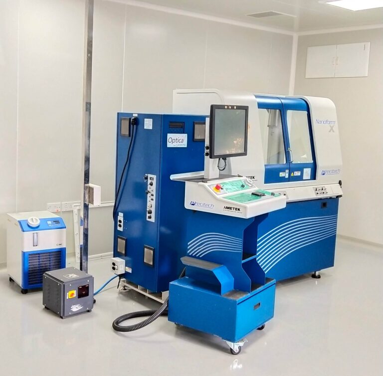
HOW SPDT IS ACHIEVED?
SPDT Process is a Near-Ideal combination of: Precision Diamond Tool of Designated Geometry, Controlled Precision Turning Operations, Deterministic Material Removal, Meticulous Machining Protocols, Detailed Dimensional Metrology and Accurate Surface Characterization
WHY SPDT IS REQUIRED?
- To Develop Optical Surfaces with Sub-Micron Form & Figure Error and Single Digit Nanometric Finish
- To Deliver Near-Theoretical Optical Performances
- To extend the Optical Performances from Spherical to Non-Spherical Surfaces
- To Develop Systems with Budgets on Weight, Volume & Foot-Print
- To Deliver Neo-Compact Precision Modules.
CAPABILITIES:
At the Diamond Turning Facility of OPTICA the following Optical Profiles can be developed:
- Flats
- Rotationally Symmetric Conic Profiles (Spherical, Oblong Elliptical, Prolate Elliptical, Parabolic,Hyperbolics)
- Off-Axial Components
- Toric Surfaces (with Fast & SlowTool Servo Accessory)
- Lenslet Arrays
- Freeform Surfaces with limited definitions
- Ultra-High Precision Mechanical Modules with definable geometries
We can process the following Materials at our Facility:
Metals:
Non-Ferrous Metals, Aluminum & Al-Alloys, Brass, Bronze, Copper & Cu-Alloys, Nickel, Electro-less Nickel, Tin, Antimony, Silver, Low-Carbon Steels & Special High-HRC Steels
IR Materials:
Germanium, Silicon, Calcium Fluoride, Zinc Sulphide, Zinc Selenide, Chalcogenide Glasses and IRG-Series
Polymers:
PMMA, Poly Carbonate, (COP) Cyclo Olefin Polymer (ZEONEX etc), Polystyrene, Poly Ether Imide, ULTEM etc.
SURFACE PROFILE QUALITY PARAMETERS:
The surface quality of the Diamond Turn-generated profile depends on the Substrate Material, Workpiece Geometry, Precision Diamond Tools deployed, Design specifications, Work-piece Applications, Operating conditions etc.
At OPTICA, we routinely develop surface profiles with better than one wavelength Power (Form) Error, λ/3 – λ/10 (PV) Figure Error, λ/20 – λ/50 (RMS) Figure Error and Finish within 2-10 nm (Ra) of Roughness.
The Profile surface quality can be tailored as per the customers’ requirements.
